EMC DEBUGGING GUILDE : REDUCE RADIATED EMISSION
Language : Vietnames
Hướng Dẫn Gỡ Lỗi EMC: Phương Pháp Tối Ưu
Hóa và Triệt Tiêu Nhiễu Bức Xạ
Trong môi trường điện tử ngày nay, việc kiểm soát phát xạ bức xạ là yếu tố quan trọng giúp đảm bảo rằng sản phẩm của bạn không gây nhiễu cho các thiết bị xung quanh và đáp ứng các tiêu chuẩn EMC nghiêm ngặt. Bài viết dưới đây sẽ cung cấp cho bạn một hướng dẫn gỡ lỗi EMC tập trung vào giảm phát xạ bức xạ, với các giải pháp thiết kế và kỹ thuật thực tiễn từ kinh nghiệm chuyên môn.
1. Hiểu Về Phát Xạ Bức Xạ
Phát xạ bức xạ là hiện tượng thiết bị điện tử phát ra sóng điện từ vào không gian, có thể gây nhiễu cho các thiết bị khác hoặc vi phạm các tiêu chuẩn EMC. Điều này đặc biệt quan trọng với các sản phẩm như thiết bị đa phương tiện, hệ thống truyền thông hay các ứng dụng công nghiệp đòi hỏi độ ổn định cao.
2. Thiết Lập Thử Nghiệm
Thử nghiệm đo nhiễu dẫn tại cổng nguồn dải tần (150 kHz - 30 MHz)2.1 Trang thiết bị sử dụng - EMI test receiver
- LISN (Two Line V Network) - Cable - 3m Anechoic chamber - PRE-AM 9 kHz - 1 GHz
2.2 Bố trí thử nghiệm

Bố trí thử nhiệm nhiễu bức xạ (CISPR 32) - Thử nghiệm được tiến hành trong buồng không phản xạ- Thử nghiệm được tiến hành ở dải tần số từ 30 MHz đến 1 GHz.- EUT được đặt trên tấm gỗ ở độ cao 0,8 m tính từ sàn- Khoảng cách EUT đên AE là 0.1 m- Khoảng cách đo từ Antenna đến EUT là 3m ,10m or 30 m
2.3 Giới hạn

Giới hạn đo nhiễu bức xạ của thiết bị đa phương tiện loại B ( CISPR 32)
2.4 Đánh giá kết quả- Kết quả tại tần số 30 MHz - 1 GHz thấp hơn giới hạn ở mục 2.3 thì sản phẩm đạt yêu cầu
Sản phẩm đã không vượt qua bài kiểm tra nhiễu bức xạ tại dải tần 30 MHz - 1 GHz

3. Các Phương Pháp Giảm Phát Xạ Bức Xạ
3.1 Ferrite core

- Sử dụng ferrite core để giảm nhiễu bức xạ
- Cách sử dụng :
- Lựa chọn ferrite core phù hợp với kích thước và quan tâm đến tại tần số nào thì trở kháng tại đó giảm bao nhiêu ?
3.2 Sử dụng bộ lọc
Nhà thiết kế có hai lựa chọn để giảm sự ghép nối dẫn. Nếu tần số nhiễu khác với tần số của tín hiệu dự định truyền qua dây dẫn, có thể sử dụng bộ lọc
3.3 Giảm nhiễu điện dung giữa 2 dây dẫn và mặt phẳng đất

Hai dây dẫn: Một dây mang điện áp V1, dây còn lại nối
với tải có trở kháng R5 và có điện áp V2
- Tăng khoảng cách giữa các dây
- Che chắn shield
- Sắp xếp dây dẫn hợp lí
- Dùng mặt phẳng tiếp địa
3.4 sử dụng RC Snubber

- Phương pháp RC Snubber là một kỹ thuật được áp dụng trong thiết kế mạch điện nhằm giảm thiểu xung điện và dao động. Bằng cách kết hợp một điện trở (R) và một tụ điện (C), RC Snubber hấp thụ và làm mờ các xung điện không mong muốn phát sinh trong quá trình chuyển mạch, từ đó giảm nhiễu EMI và bảo vệ các thành phần khác trong mạch khỏi các tác động tiêu cực. Đây là một giải pháp hiệu quả để cải thiện hiệu suất và độ tin cậy của hệ thống điện tử.
3.5 Sử dụng Snubber capacitor

- Điều này không chỉ giúp giảm nhiễu điện từ (EMI) mà còn bảo vệ các thành phần nhạy cảm khỏi sự tăng quá áp. Thông thường, điện tụ snubber được mắc song song với thiết bị chuyển mạch hoặc tải để tối ưu hóa hiệu suất mạch và nâng cao độ tin cậy chung.
Link
3.6 Sử dụng điện trở nối đất

- Việc sử dụng điện trở nối đất có thể giúp giảm EMI bằng cách tạo ra một đường dẫn ổn định cho các tín hiệu nhiễu và hạn chế các dao động không mong muốn. Tuy nhiên, mức giảm EMI phụ thuộc vào nhiều yếu tố như thiết kế mạch, giá trị điện trở, và cách bố trí PCB. Trong một số trường hợp, nếu được tối ưu hóa kỹ lưỡng, có thể đạt được mức giảm khoảng 3-10 dB, nhưng con số cụ thể chỉ có thể được xác định qua thử nghiệm và đánh giá thực tế của từng hệ thống
Link
3.7 Sử dụng tụ bypass or decoupling

Link
3.7 Sử dụng ferrite bead

- Ferrite bead là một thành phần hữu hiệu được sử dụng để giảm nhiễu EMI, đặc biệt là ở tần số cao. Khi mắc vào dây dẫn hoặc cáp, ferrite bead hoạt động như một bộ lọc tần số cao, chặn các tín hiệu nhiễu không mong muốn và hạn chế sự lan truyền của chúng. Điều này giúp cải thiện chất lượng tín hiệu và ổn định hoạt động của mạch. Việc lựa chọn ferrite bead phù hợp về giá trị cảm kháng (impedance) và cách bố trí trên PCB hoặc dây dẫn là rất quan trọng để đạt được hiệu quả lọc nhiễu tối ưu.
Link
3.7 Sử dụng che chắn

- Che chắn nhiễu là giải pháp then chốt trong thiết kế mạch điện tử nhằm giảm thiểu sóng điện từ không mong muốn. Nó sử dụng các vật liệu dẫn điện (như kim loại, hợp kim) để hấp thụ và phản xạ sóng, bảo vệ linh kiện nhạy cảm và duy trì ổn định cho mạch. Kết hợp với thiết kế PCB tối ưu và các biện pháp lọc EMI, che chắn nhiễu giúp đảm bảo sản phẩm tuân thủ tiêu chuẩn EMC và nâng cao hiệu suất vận hành.
Link
3.7 Sắp xếp bố trí thay đổi giá trị của linh kiện
- Đây là một kỹ thuật tối ưu hóa thiết kế PCB, trong đó việc điều chỉnh vị trí, khoảng cách giữa các linh kiện và cách dẫn mạch có thể làm thay đổi các giá trị điện dung, cuộn cảm gián tiếp (parasitic) của mạch. Qua đó, phương pháp này giúp giảm nhiễu, cải thiện hiệu suất của hệ thống và hỗ trợ đạt được các yêu cầu EMC nghiêm ngặt.
Link
Kết Luận
Giảm phát xạ bức xạ là một bước quan trọng trong quá trình gỡ lỗi EMC, giúp tối ưu hóa thiết kế và đảm bảo sản phẩm hoạt động ổn định trong môi trường điện từ phức tạp. Bằng cách áp dụng các giải pháp như tối ưu bố trí PCB, sử dụng màn che, bộ lọc EMI, và RC Snubber, bạn có thể cải thiện đáng kể khả năng chống nhiễu của sản phẩm.
Hãy bắt đầu áp dụng các chiến lược này vào quá trình thiết kế của bạn và biến mỗi thách thức EMC thành cơ hội để tạo ra sản phẩm chất lượng và cạnh tranh hơn trên thị trường.
Nếu bạn muốn tìm hiểu thêm chi tiết và nhận được các mẹo kỹ thuật hữu ích, hãy liên hệ với chúng tôi để được tư vấn và nhận tài liệu miễn phí.
Nếu bạn thấy bài viết hữu ích, hãy CHIA SẺ và để lại BÌNH LUẬN – phản hồi của bạn chính là động lực để chúng tôi tiếp tục mang đến những nội dung giá trị.
Cảm ơn bạn đã ủng hộ!
— GCL HCM
References:
[1] International Special Committee on Radio Interference, CISPR 32:2015 – Electromagnetic Compatibility of Multimedia Equipment – Emission Requirements, and CISPR 35:2015 – Electromagnetic Compatibility Measurement Techniques for Multimedia Equipment, 2015.
[2] System Design and Layout Techniques for Noise Reduction in
MCU-Based Systems, Freescale Application Note, AN1259.
[3] Determining MCU Oscillator Start-up Parameters,
Freescale Application Note, AN1783.
[4] Resetting Microcontrollers During Power Transitions,
Freescale Application Note, AN1744.
[5] Resetting MCUs, Freescale Engineering Bulletin, EB413.
[6] Trends in EMC Testing of Household Appliances,
SCHAFFNER Application Note, SAN014.
[7] EMC at Component and PCB Level,
Martin O’Hara, Newnes, 1998.
-----------------------------------------------------------------------------------------------------------------------------
Language : English
EMC Debugging Guide: Techniques for
Optimizing and Suppressing Radiated Emissions
In today's electronic environment, controlling radiated emissions is a critical factor in ensuring that your product does not interfere with surrounding devices and complies with strict EMC standards. The following article provides an EMC debugging guide focused on reducing radiated emissions, featuring design solutions and practical techniques based on professional experience.
1. Understanding Radiated Emissions
Radiated emissions refer to the phenomenon where an electronic device emits electromagnetic waves into the surrounding space, which can interfere with other devices or violate EMC standards. This is particularly important for products such as multimedia equipment, communication systems, and industrial applications that require high stability..
2. 2. Test Setup
Radiated Emisson Test 30 MHz - 1 GHz2.1 Equipmnet use - EMI test receiver
- LISN (Two Line V Network) - Cable - 3m Anechoic chamber - PRE-AM 9 kHz - 1 GHz
2.2 Test setup
Radiated emission test setup follow (CISPR 32) - Testing is conducted in an anechoic chamber.- The test is performed over a frequency range from 30 MHz to 1 GHz.
- The Equipment Under Test (EUT) is placed on a wooden panel at a height of 0.8 m from the floor.
- The distance between the EUT and the AE is 0.1 m.
- The measurement distance from the antenna to the EUT is 3 m, 10 m, or 30 m
2.3 Limit
Limits for measurement of radiated disturbances for class B multimedia equipment (CISPR 32)
2.4 Evaluate the results- The result at frequency 30MHz - 1 GHz is lower than the limit in section 2.3, the product meets the requirements.
The product has failed the radiated interference test at the frequency range of 30 MHz - 1 GHz.
- The test is performed over a frequency range from 30 MHz to 1 GHz.
- The Equipment Under Test (EUT) is placed on a wooden panel at a height of 0.8 m from the floor.
- The distance between the EUT and the AE is 0.1 m.
- The measurement distance from the antenna to the EUT is 3 m, 10 m, or 30 m
3. Methods of Reducing Radiation Emission
3.1 Ferrite core
Use ferrite core to reduce radiation noise
How to use:
- Wrap 1 turn, 2 turns or thread the wire through the input and output of the circuit
- Choose ferrite core suitable for size and pay attention to at what frequency the impedance is reduced by how much?
Click on the link below for more details on how to use ferrite core
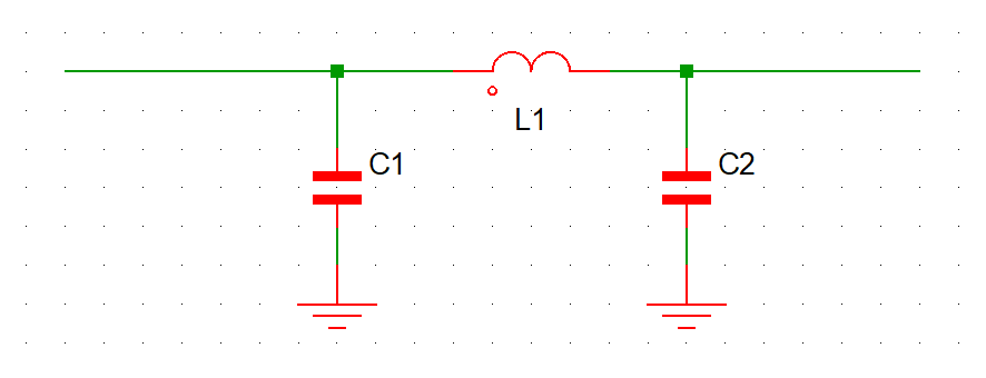
3.2 Use LC filter
Designers have two options to reduce conductive coupling. If the interference frequency is different from the frequency of the intended signal transmitted through the conductor, a filter can be used.
Click on the link below for more details on how to use ferrite core
3.3 Reduce the interference between the two conductors and the ground plane.
Two conductors: One carries voltage V1, the other is connected to a load with impedance R5 and voltage V2
Each conductor has parasitic capacitance to ground, respectively C3 and C4
Method:
- Increase the spacing between wires
- Use shielding
- Arrange wiring properly
- Use a ground plane
Click on the link below for more details on how to use ferrite core
3.4 Use RC Snubber
- The RC Snubber method is a technique applied in circuit design to minimize voltage spikes and oscillations. By combining a resistor (R) and a capacitor (C), the RC Snubber absorbs and dampens unwanted voltage spikes generated during switching, thereby reducing EMI and protecting other components in the circuit from adverse effects. This is an effective solution for enhancing the performance and reliability of electronic systems.
Click on the link below for more details on how to use ferrite core
3.5 Use Snubber capacitor
- Điều này không chỉ giúp giảm nhiễu điện từ (EMI) mà còn bảo vệ các thành phần nhạy cảm khỏi sự tăng quá áp. Thông thường, điện tụ snubber được mắc song song với thiết bị chuyển mạch hoặc tải để tối ưu hóa hiệu suất mạch và nâng cao độ tin cậy chung.
Click on the link below for more details on how to use ferrite core
3.6 Sử dụng điện trở nối đất
- Using a ground resistor can help reduce EMI by providing a stable path for noise signals and limiting unwanted oscillations. However, the level of EMI reduction depends on various factors such as circuit design, resistor value, and PCB layout. In some cases, if optimized thoroughly, a reduction of approximately 3-10 dB can be achieved, but the exact value can only be determined through testing and practical evaluation of each system.
Click on the link below for more details on how to use ferrite core
3.7 Use bypass or decoupling cap
- Bypass capacitors (or decoupling capacitors) are essential components that help filter and reduce high-frequency noise in electronic circuits. Placed in parallel between the power supply and ground, bypass capacitors provide a low-impedance path for noise signals, helping stabilize the supply voltage for ICs and sensitive components. Positioning these capacitors near critical components enhances circuit performance, reduces EMI, and increases overall system stability. The capacitor values are typically chosen from a few nF to several µF, depending on the specific circuit requirements
Click on the link below for more details on how to use ferrite core
3.7 Use ferrite bead
- Ferrite beads are effective components used to reduce EMI, especially at high frequencies. When attached to wires or cables, ferrite beads act as high-frequency filters by blocking unwanted noise signals and limiting their propagation. This improves signal quality and stabilizes circuit operation. Choosing the right ferrite bead with the appropriate impedance value and placing it correctly on the PCB or wiring is crucial for optimal noise filtering performance.
Click on the link below for more details on how to use ferrite core
3.7 Using Shielding
- EMI shielding is a key solution in electronic circuit design aimed at minimizing unwanted electromagnetic waves. It uses conductive materials (such as metals and alloys) to absorb and reflect these waves, protecting sensitive components and maintaining circuit stability. Combined with optimized PCB design and EMI filtering measures, shielding helps ensure that products comply with EMC standards and enhances overall operational performance.
Link
Click on the link below for more details on how to use ferrite core
3.7 Arrangement and Adjustment of Component Values
- This is a PCB design optimization technique where adjusting the position, spacing between components, and trace routing can change the circuit’s parasitic capacitance and inductance. This method helps reduce noise, improve system performance, and support strict EMC compliance.
Click on the link below to learn more about these methods.
Click on the link below for more details on how to use ferrite core
Conclusion
Reducing radiated emissions is a critical step in EMC debugging—it optimizes design and ensures products operate stably in complex electromagnetic environments. By applying solutions such as optimized PCB layout, EMI shielding, EMI filters, and RC snubbers, you can significantly enhance your product’s noise immunity.
Start applying these strategies in your design process and turn every EMC challenge into an opportunity to create higher-quality and more competitive products.
If you’d like to learn more details and receive valuable technical tips, please contact us for consultation and to receive free documentation.
If you find this article useful, please SHARE and leave a COMMENT—your feedback is the motivation that drives us to continue delivering valuable content.
Thank you for your support!
— GCL HCM
References:
[1] International Special Committee on Radio Interference, CISPR 32:2015 – Electromagnetic Compatibility of Multimedia Equipment – Emission Requirements, and CISPR 35:2015 – Electromagnetic Compatibility Measurement Techniques for Multimedia Equipment, 2015.
[2] System Design and Layout Techniques for Noise Reduction in
MCU-Based Systems, Freescale Application Note, AN1259.
[3] Determining MCU Oscillator Start-up Parameters,
Freescale Application Note, AN1783.
[4] Resetting Microcontrollers During Power Transitions,
Freescale Application Note, AN1744.
[5] Resetting MCUs, Freescale Engineering Bulletin, EB413.
[6] Trends in EMC Testing of Household Appliances,
SCHAFFNER Application Note, SAN014.
[7] EMC at Component and PCB Level,
Martin O’Hara, Newnes, 1998.
#EMC #EMCTesting #ElectromagneticCompatibility #EMIMitigation #ConductedEmission #RadiatedEmission #EMCStandards #IEC61000 #CISPR #PCBDebugging #SignalIntegrity #NoiseReduction #FerriteCore #EMCDebugging #FireAlarmEMC #ConductedSusceptibility #EMCSolutions #ShieldingTechniques #PCBDesignForEMC #PowerLineNoise #ElectromagneticInterference #ESDTesting #RFInterference #IndustrialEMC #ElectronicDesign #EMCCompliance #NoiseFiltering #GroundingTechniques #ElectronicsTesting #EMCRegulations #EMCConsulting #EMCFailureAnalysis


Nhận xét
Đăng nhận xét