Demo Project 2 : Debugging radiated emission for LED
Gỡ lỗi EMC Cho Đèn LED
1. Giới thiệu
Trong quá trình thiết kế và sản xuất thiết bị điện tử, đặc biệt là các sản phẩm chiếu sáng như đèn LED, đảm bảo Tương thích điện từ (EMC) là một bước quan trọng để sản phẩm vận hành ổn định và không gây nhiễu đến các thiết bị xung quanh. Việc kiểm soát phát xạ bức xạ giúp đảm bảo sản phẩm tuân thủ các tiêu chuẩn EMC quốc tế, tránh các rủi ro về pháp lý và kỹ thuật.
Báo cáo này sẽ tập trung vào quy trình gỡ lỗi EMC cho mạch driver của đèn LED, đặc biệt là việc giảm thiểu phát xạ bức xạ (Radiated Emission) thông qua các kỹ thuật thiết kế tối ưu và giải pháp thực tế.
2. Mục tiêu
Quy trình này nhằm hướng đến các mục tiêu cụ thể sau:
Xác định các nguồn phát xạ EMI chủ yếu trong mạch driver LED, bao gồm:
Chân Drain của IC chuyển mạch.
Đầu vào (Input) và đầu ra (Output) của mạch driver.
Vùng xung quanh diode và mạch snubber.
Đánh giá mức độ phát xạ bức xạ của mạch LED theo tiêu chuẩn EMC hiện hành, đặc biệt là tiêu chuẩn:
CISPR 15 / EN 55015: dành cho thiết bị chiếu sáng.
Đề xuất và triển khai các biện pháp khắc phục nhằm giảm thiểu phát xạ bức xạ, giúp sản phẩm đạt tiêu chuẩn EMC, đồng thời tối ưu chi phí và không gian mạch.3. Phương pháp thực hiện
3.1. Thiết lập môi trường thử nghiệm
Môi trường thử nghiệm: tiến hành trong buồng không phản xạ (Anechoic Chamber) để loại bỏ các nguồn nhiễu bên ngoài.
Dải tần kiểm tra: 30 MHz đến 1 GHz.
Thiết bị thử nghiệm:
Máy phân tích phổ (Spectrum Analyzer).
Ăng-ten đo (Antenna) cho thử nghiệm phát xạ bức xạ.
Vị trí thiết bị kiểm thử (EUT - Equipment Under Test):
EUT được đặt trên một tấm gỗ cách sàn 0,8 m.
Khoảng cách đo từ ăng-ten đến EUT: 3 m, 10 m hoặc 30 m tùy theo yêu cầu của tiêu chuẩn CISPR 15.
3.2. Đo lường và phân tích
Kết nối: Dùng đầu dò từ trường gần (Near-field Probe) kết hợp với Spectrum Analyzer để dò tìm nguồn phát xạ lớn nhất.
Thu thập dữ liệu:
Đo tín hiệu tại các vị trí: đầu vào, đầu ra, và khu vực quanh IC chuyển mạch.
Ghi lại mức phát xạ bức xạ theo từng tần số.
So sánh:
Đối chiếu dữ liệu đo được với giới hạn phát xạ quy định trong tiêu chuẩn CISPR 15 / EN 55015.
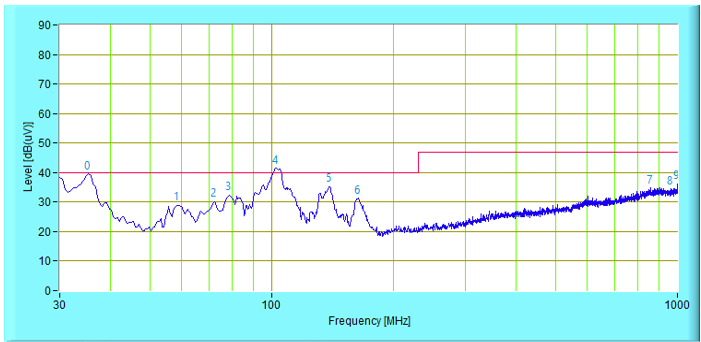
Sau khi thực hiện bài kiểm tra đo nhiễu bức xạ tại dãi tần 30 MHz - 1 GHz :
Dữ liệu ban đầu thu được :

3.3. Triển khai giải pháp khắc phục:
- Ban đầu ta dự đoán nơi có thể phát sinh nguồn nhiễu cao
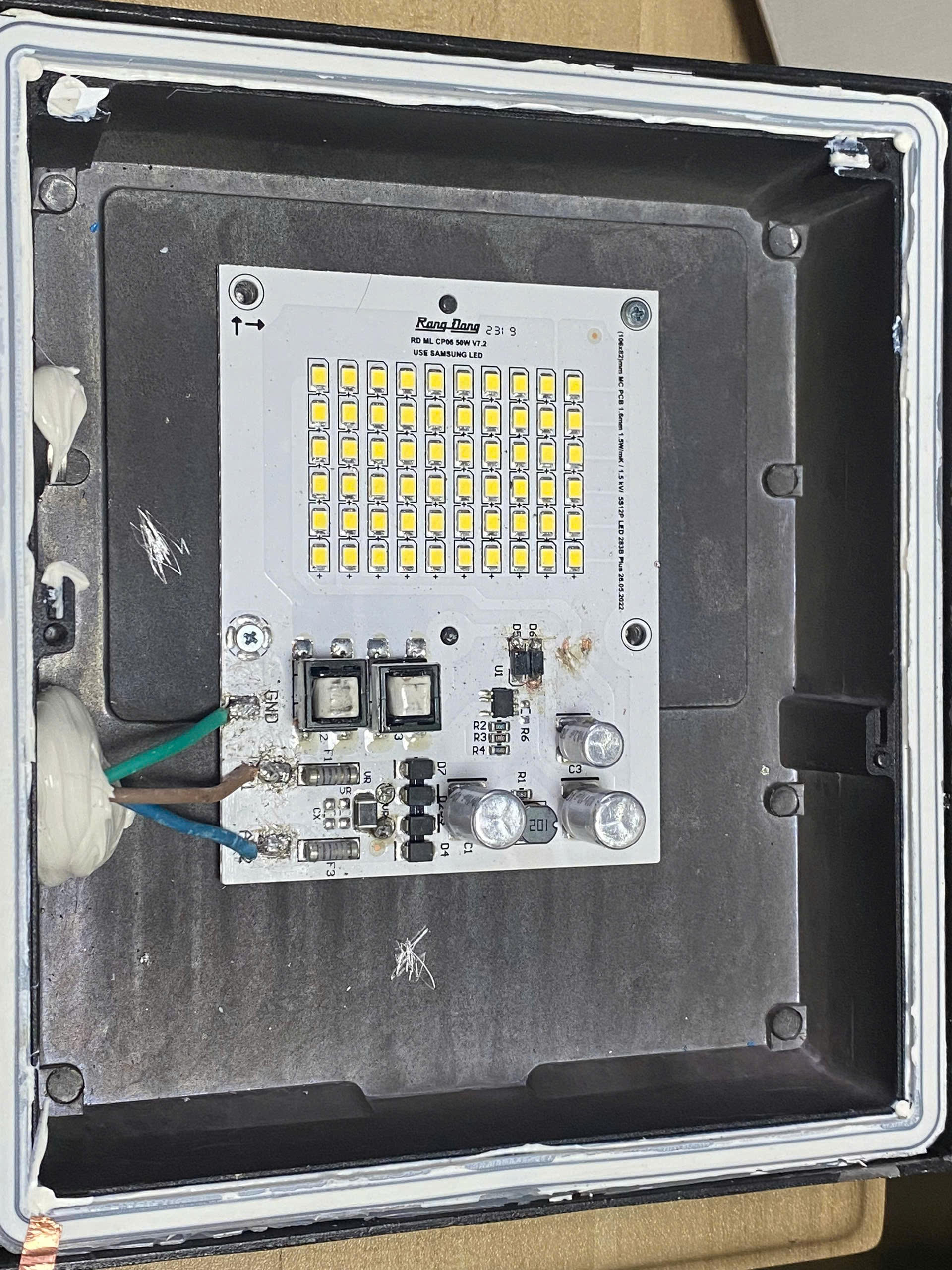

Nhiễu cao có thể xuất hiện tại Input ,Output or IC chuyển mạch area 1,2 or 3


Kiểm tra bằng cách kết nối đầu dò với Spectrum để tìm ra nơi có nhiễu hoạt động mạnh nhất
Sau khi dò tại các vùng nghi ngờ và ta thấy xung nhiễu hoạt động mạnh nhất tại IC chuyển mạch
4. Các trường hợp gỡ lỗi thực tế
TH 0 : Mạch ban đầu của nhà sản xuất


Kết quả
TH 2: Thêm ferrite core 1 vòng tai Output của mạch driver L N


Kết quả
Kết quả
TH 6:Thêm tụ snubber vào đầu diode tại IC chuyển mạch

TH 7:Thêm ferrite core 2 vòng tai Output của mạch driver L N
Thêm tụ snubber vào đầu diode tại IC chuyển mạch


5. Đánh giá và kết luận
Đánh giá :
Sau 7 trường hợp thử nghiệm nhận ra rằng :
- Tại trường hợp 1,2,3,4,5,6 sản phẩm chưa đạt .
- Trường hợp 7: Thêm ferrite core 2 vòng tai Output của mạch driver L N và thêm tụ snubber vào đầu diode tại IC chuyển mạch
Kết luận:
Bằng cách kết hợp các giải pháp thiết kế và kỹ thuật hiện đại, việc gỡ lỗi EMC đã đạt được kết quả khả quan, giúp sản phẩm hoạt động ổn định và đáp ứng các tiêu chuẩn quốc tế. Quá trình này không chỉ cải thiện hiệu suất mà còn là cơ hội để tối ưu hóa thiết kế cho các dự án tương lai.
Báo cáo này được biên soạn bởi đội ngũ kỹ sư của GCL HCM nhằm chia sẻ kinh nghiệm và kiến thức trong lĩnh vực EMC debugging
Nếu bạn muốn tìm hiểu thêm chi tiết và nhận được các mẹo kỹ thuật hữu ích, hãy liên hệ với chúng tôi để được tư vấn và nhận tài liệu miễn phí.
Hoăc nhấn vào Link bên dưới để tham khảo những biện pháp giảm nhiễu bức xạ khác
Nếu bạn thấy bài viết hữu ích, hãy CHIA SẺ và để lại BÌNH LUẬN – phản hồi của bạn chính là động lực để chúng tôi tiếp tục mang đến những nội dung giá trị.
Cảm ơn bạn đã ủng hộ!
— GCL HCM
Thông tin liên hệ :
EMC Team
SĐT : 0357515079 - 098 546 68 50
Email : khuongpham747@gmail.com - dangnghia06@gmail.com
Công ty : EMC Debugging Center - GCL HCM
References:
[1] International Special Committee on Radio Interference, CISPR 32:2015 – Electromagnetic Compatibility of Multimedia Equipment – Emission Requirements, and CISPR 35:2015 – Electromagnetic Compatibility Measurement Techniques for Multimedia Equipment, 2015.
[2] System Design and Layout Techniques for Noise Reduction in
MCU-Based Systems, Freescale Application Note, AN1259.
[3] Determining MCU Oscillator Start-up Parameters,
Freescale Application Note, AN1783.
[4] Resetting Microcontrollers During Power Transitions,
Freescale Application Note, AN1744.
[5] Resetting MCUs, Freescale Engineering Bulletin, EB413.
[6] Trends in EMC Testing of Household Appliances,
SCHAFFNER Application Note, SAN014.
[7] EMC at Component and PCB Level,
Martin O’Hara, Newnes, 1998.
----------------------------------------------------------------------------------------------------------------------------
EMC DEBUGGING FOR LED DRIVERS
1. Introduction
During the design and manufacturing of electronic devices, especially lighting products like LED drivers, ensuring Electromagnetic Compatibility (EMC) is crucial to guarantee stable operation without interfering with surrounding devices. Controlling radiated emissions not only ensures compliance with international EMC standards but also mitigates legal and technical risks.
This report focuses on the EMC debugging process for LED driver circuits, specifically addressing radiated emission reduction through optimized design techniques and practical solutions.
2. Objectives
The process aims to achieve the following objectives:
Identify major EMI sources in the LED driver circuit, including:
The Drain pin of the switching IC.
Input and output terminals of the driver circuit.
Areas surrounding the diode and snubber circuit.
Evaluate radiated emission levels of the LED circuit according to current EMC standards, particularly:
CISPR 15 / EN 55015: for lighting equipment.
Propose and implement corrective measures to reduce radiated emissions, ensuring compliance with EMC standards while optimizing cost and circuit space.
3. Methodology
3.1. Test Environment Setup
Test environment: Conducted in an Anechoic Chamber to eliminate external noise sources.
Test frequency range: 30 MHz to 1 GHz.
Testing equipment:
Spectrum Analyzer for measuring emission levels.
Antenna for radiated emission testing.
Device Under Test (DUT) placement:
DUT placed on a wooden table 0.8 m above the ground.
Measurement distance from antenna to DUT: 3 m, 10 m, or 30 m depending on CISPR 15 requirements.
3.2. Measurement and Analysis
Connection setup: Use a Near-field Probe connected to a Spectrum Analyzer to locate the strongest emission sources.
Data collection:
Measure signals at input, output, and areas around the switching IC.
Record radiated emission levels across different frequencies.
Comparison:
Compare the measured data against the radiated emission limits specified in CISPR 15 / EN 55015.
Initial Data Collected:
3.3. Implementation of Mitigation Solutions:
- Initially, we predicted potential areas where high levels of noise could originate.
- Test by connecting the probe to the Spectrum to find out where the noise is strongestAfter probing in the suspected areas and we found the strongest noise pulse at the switching IC
4. Practical Debugging Cases
Case 0: The original circuit from the manufacturer.
Test result
Case 2: Added a ferrite core with one turn at the Output of the driver (L, N).
Test result
Test result
Case 6: Added a snubber capacitor to the diode at the switching IC.
Case 7: Added a ferrite core with two turns at the Output of the driver (L, N) and a snubber capacitor to the diode at the switching IC.
5. Evaluation and Conclusion
Evaluation:
After testing all 7 scenarios, the following results were observed:
In Cases 1, 2, 3, 4, 5, 6, the product did not pass EMC standards.
In Case 7: Combining 2-turn ferrite core at the driver output (L, N) and snubber capacitor at the diode of the switching IC yielded promising results, ensuring the product met the radiated emission limits according to CISPR 15.
Conclusion:
By combining modern design strategies and technical solutions, the EMC debugging process achieved positive results, allowing the product to operate stably and comply with international standards. This process not only improved performance but also provided opportunities to optimize designs for future projects.
This report was prepared by the engineering team at GCL HCM to share insights and knowledge in EMC debugging.
If you want to learn more and receive valuable technical tips, please contact us for consultation and free materials.
Or click the Link below to explore additional radiated emission reduction methods.
If you found this article helpful, please SHARE and leave a COMMENT – your feedback motivates us to continue delivering high-value content.
Thank you for your support!
— GCL HCM
EMC Team
Phone: SĐT : 0357515079 - 098 546 68 50
Email : khuongpham747@gmail.com - dangnghia06@gmail.com
Company: EMC Debugging Center - GCL HCM
References:
[1] International Special Committee on Radio Interference, CISPR 32:2015 – Electromagnetic Compatibility of Multimedia Equipment – Emission Requirements, and CISPR 35:2015 – Electromagnetic Compatibility Measurement Techniques for Multimedia Equipment, 2015.
[2] System Design and Layout Techniques for Noise Reduction in
MCU-Based Systems, Freescale Application Note, AN1259.
[3] Determining MCU Oscillator Start-up Parameters,
Freescale Application Note, AN1783.
[4] Resetting Microcontrollers During Power Transitions,
Freescale Application Note, AN1744.
[5] Resetting MCUs, Freescale Engineering Bulletin, EB413.
[6] Trends in EMC Testing of Household Appliances,
SCHAFFNER Application Note, SAN014.
[7] EMC at Component and PCB Level,
Martin O’Hara, Newnes, 1998.
#EMC #EMCTesting #ElectromagneticCompatibility #EMIMitigation #ConductedEmission #RadiatedEmission #EMCStandards #IEC61000 #CISPR #PCBDebugging #SignalIntegrity #NoiseReduction #FerriteCore #EMCDebugging #FireAlarmEMC #ConductedSusceptibility #EMCSolutions #ShieldingTechniques #PCBDesignForEMC #PowerLineNoise #ElectromagneticInterference #ESDTesting #RFInterference #IndustrialEMC #ElectronicDesign #EMCCompliance #NoiseFiltering #GroundingTechniques #ElectronicsTesting #EMCRegulations #EMCConsulting #EMCFailureAnalysis


Nhận xét
Đăng nhận xét