Demo Project 4 : Debugging Conducted Emisison For SMPS Circuit
EMC Debugging : Conducted Emission Test for
SMPS Circuit
1. Introduction
In the design and manufacturing of electronic devices, ensuring electromagnetic compatibility (EMC) is a key factor in maintaining stable product operation and preventing interference with other systems. This report presents the EMC debugging process for the product, focusing on reducing conducted emissions and improving performance through optimized design solutions and advanced techniques.
2. Objectives
- Identify EMI noise sources caused by conducted emissions at the power port.
- Evaluate the emission levels of the product according to EMC standards, depending on the type of device using the SMPS.
- Implement corrective measures to reduce emissions, thereby enhancing the product’s stability and performance.
3. Methodology :
3.1. Test Environment Setup
- The test is conducted in a shielded test environment to minimize external interference.
- Test frequency range: 150 kHz - 30 MHz.
- The Equipment Under Test (EUT) is connected to a Line Impedance Stabilization Network (LISN) to measure conducted emissions at the power port.
- Measuring equipment includes a Spectrum Analyzer and specialized EMC analysis software.
3.2. Measurement and Analysis
- A Spectrum Analyzer combined with LISN is used to collect conducted emission data from the power line.
- The obtained data is compared with the emission limits specified in CISPR 15 (for lighting equipment), CISPR 32 (for multimedia equipment), or CISPR 11 (for industrial equipment), depending on the SMPS application.
- After performing the conducted emission test within the 150 kHz - 30 MHz range, the initial data showed some noise peaks exceeding the specified limits at frequency X kHz/Y MHz..
Initial Data Collected:


Note : Attenuator 6 dB
3.3. Implementation of Corrective Solutions
In this circuit we see common mode filter

L = 56.7 uH à Fc = 450 kHz
Cy = 2.2 n
Fc = 450 kHz
In theory, to filter out noise at high frequencies from 150
kHz and above, we need to set the cutoff frequency at 15 kHz to cut frequency
at 150 kHz à
Fc= 450 kHz not qualified
Method : Common Mode Filter Design
When we conducted emission test : High noise at 0.15 MHz – 6
MHz
Chooose cut frequency at 15 kHz to cut noise at 150 kHz
L_cm = 10 mH because
we don't use the inductor in differential mode, we take L_dm = L_cm or more
precisely, L_dm = 1/2L_cd to calculate
the capacitor value Cx
The common-mode inductor consists of two symmetrical coils on the same core.
When considering differential mode, the current passes through the two coils in
opposite directions, reducing the total magnetic flux in the core.This reduces
the total resistance to almost half the value
L_dm = 10 mH or L_dm = 5 mH.

4. Real-World Debugging Cases
Case 0: Manufacturer’s Original Circuit
4. Real-World Debugging Cases
Case 0: Manufacturer’s Original Circuit
Reference ResultAtt = 60 dBAmpe = 1.5 AC-X1 = 2200 pFCase 1: Change Y-Cap = 2200 pF ==> 10000 pF

Kết quả
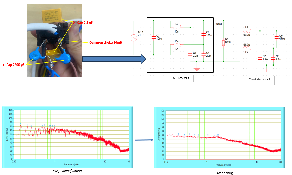
Case 2: Add EMI filter Cx= 0.1 uF, Cy = 2200 pF ,Choke = 10 mH

Kết quả 5. Evaluation and Conclusion
Evaluation:
After conducting two test cases, the following observations were made:
- In Case 1, the product did not meet the required standards.
- In Case 2, the test results successfully met the compliance requirements.
→ The optimized solution from Case 2 is selected.
Kết quả
Case 2: Add EMI filter Cx= 0.1 uF, Cy = 2200 pF ,Choke = 10 mH
Kết quả
5. Evaluation and Conclusion
Evaluation:
After conducting two test cases, the following observations were made:
- In Case 1, the product did not meet the required standards.
- In Case 2, the test results successfully met the compliance requirements.
→ The optimized solution from Case 2 is selected.
Conclusion:
By applying advanced design solutions and modern techniques, the EMC debugging process has delivered positive results, ensuring stable product operation and compliance with international standards. Beyond improving performance, this process also creates opportunities for design optimization, laying a solid foundation for future projects.
This report was compiled by the GCL HCM Engineering Team to share practical experience and knowledge in EMC debugging.
If you want to learn more or receive useful technical tips, please contact us for free consultation and resources.
Or click the link below to explore other methods for reducing radiated emissions:
If you find this article helpful, please SHARE and leave a COMMENT — your feedback motivates us to continue delivering valuable content!
Thank you for your support!
— GCL HCM
Contact information:
EMC Team
Telephone : 035 751 50 79 - 098 546 68 50
Email : khuongpham747@gmail.com - dangnghia06@gmail.com
Company: EMC Debugging Center - GCL HCM
Reference
[1] International Special Committee on Radio Interference, CISPR 32:2015 – Electromagnetic Compatibility of Multimedia Equipment – Emission Requirements, and CISPR 35:2015 – Electromagnetic Compatibility Measurement Techniques for Multimedia Equipment, 2015.
[2] System Design and Layout Techniques for Noise Reduction in
MCU-Based Systems, Freescale Application Note, AN1259.
[3] Determining MCU Oscillator Start-up Parameters,
Freescale Application Note, AN1783.
[4] Resetting Microcontrollers During Power Transitions,
Freescale Application Note, AN1744.
[5] Resetting MCUs, Freescale Engineering Bulletin, EB413.
[6] Trends in EMC Testing of Household Appliances,
SCHAFFNER Application Note, SAN014.
[7] EMC at Component and PCB Level,
Martin O’Hara, Newnes, 1998.
-----------------------------------------------------------------------------------------------------------------------------
Gỡ lỗi EMC Cho mạch SMPS
1. Giới thiệu
Trong quá trình thiết kế và sản xuất thiết bị điện tử, đảm bảo tương thích điện từ (EMC) là yếu tố then chốt để sản phẩm hoạt động ổn định và không gây nhiễu cho các hệ thống khác. Báo cáo này trình bày quá trình gỡ lỗi EMC cho sản phẩm, tập trung vào việc giảm phát xạ dẫn (Conducted Emission) và cải thiện hiệu suất hoạt động thông qua các giải pháp thiết kế và kỹ thuật tối ưu.
2. Mục tiêu
Xác định các nguồn nhiễu EMI gây ra bởi phát xạ dẫn tại cổng nguồn.
Đánh giá mức độ phát xạ của sản phẩm theo tiêu chuẩn EMC, tùy thuộc vào loại thiết bị sử dụng nguồn SMPS.
Triển khai các biện pháp khắc phục để giảm phát xạ, từ đó cải thiện độ ổn định và hiệu suất của sản phẩm.
3. Phương pháp thực hiện
3.1. Thiết lập môi trường thử nghiệm:
Thử nghiệm được tiến hành trong môi trường kiểm tra được che chắn để giảm thiểu nhiễu ngoại lai.
Dải tần kiểm tra: 150 kHz - 30 MHz.
EUT (Equipment Under Test) được kết nối với LISN (Line Impedance Stabilization Network) để đo nhiễu dẫn tại cổng nguồn.
Các thiết bị đo bao gồm máy phân tích phổ (Spectrum Analyzer) và phần mềm phân tích EMC chuyên dụng.
3.2. Đo lường và phân tích:
Sử dụng máy phân tích phổ kết hợp với LISN để thu thập dữ liệu phát xạ dẫn trên dây nguồn.
So sánh dữ liệu thu được với giới hạn phát xạ theo tiêu chuẩn CISPR 15 (cho thiết bị chiếu sáng), CISPR 32 (cho thiết bị đa phương tiện), hoặc CISPR 11 (cho thiết bị công nghiệp), tùy vào ứng dụng của nguồn SMPS.
Sau khi thực hiện bài kiểm tra nhiễu dẫn tại dải tần 150 kHz - 30 MHz, dữ liệu ban đầu thu được cho thấy một số đỉnh nhiễu vượt mức giới hạn quy định tại tần số X kHz/Y MHz.
Dữ liệu ban đầu thu được :
Note : Attenuator 6 dB
3.3. Triển khai giải pháp khắc phục:
Trong mạch này, chúng ta thấy bộ lọc mode chung (Common Mode Filter).
L = 56,7 µH → Fc = 450 kHz
Cy = 2,2 nF
Fc = 450 kHz
Về mặt lý thuyết, để lọc nhiễu ở tần số cao từ 150 kHz trở lên, chúng ta cần đặt tần số cắt ở 15 kHz để loại bỏ nhiễu tại 150 kHz. → Fc = 450 kHz không đạt yêu cầu.
Thiết kế bộ lọc EMI filter :
Khi thực hiện thử nghiệm phát xạ dẫn (Conducted Emission Test):
Nhiễu cao tại 0,15 MHz – 6 MHz.
Chọn tần số cắt 15 kHz để lọc nhiễu tại 150 kHz.
- L_cm = 10 mH vì chúng ta không sử dụng cuộn cảm ở chế độ vi sai (Differential Mode).
- Lấy L_dm = L_cm hoặc chính xác hơn L_dm = 1/2 L_cm để tính giá trị tụ Cx.
Cuộn cảm mode chung gồm hai cuộn dây đối xứng trên cùng một lõi. Khi xét ở chế độ vi sai, dòng điện đi qua hai cuộn dây theo hướng ngược nhau, làm giảm tổng từ thông trong lõi. Điều này làm giảm tổng trở kháng xuống gần một nửa giá trị ban đầu.
L_dm = 10 mH hoặc L_dm = 5 mH.
4. Các trường hợp gỡ lỗi thực tế
TH 0 : Mạch ban đầu của nhà sản xuất
4. Các trường hợp gỡ lỗi thực tế
TH 0 : Mạch ban đầu của nhà sản xuất
Tham chiếu Kết quả ban đầu Att = 60 dBAmpe = 1.5 AC-X1 = 2200 pFTH 1: Thay Y-Cap = 2200 pF ==> 10000 pF
Kết quả
TH 2: Thêm bộ lọc EMI filter Cx= 0.1 uF, Cy = 2200 pF ,Choke = 10 mH
Kết quả 5. Đánh giá và kết luận
Đánh giá :
Sau 2 trường hợp thử nghiệm nhận ra rằng :
- Tại trường hợp 1 sản phẩm chưa đạt
- Tại trường hợp 2 kết quả thử nghiệm đã đạt
----->Ta chọn phương án số 2
Kết luận:
Nhờ áp dụng các giải pháp thiết kế tiên tiến và kỹ thuật hiện đại, quá trình gỡ lỗi EMC đã mang lại kết quả tích cực, đảm bảo sản phẩm hoạt động ổn định và tuân thủ các tiêu chuẩn quốc tế. Không chỉ giúp nâng cao hiệu suất, quá trình này còn mở ra cơ hội tối ưu hóa thiết kế, tạo nền tảng vững chắc cho các dự án trong tương lai
Báo cáo này được biên soạn bởi đội ngũ kỹ sư của GCL HCM nhằm chia sẻ kinh nghiệm và kiến thức trong lĩnh vực EMC debugging
Nếu bạn muốn tìm hiểu thêm chi tiết và nhận được các mẹo kỹ thuật hữu ích, hãy liên hệ với chúng tôi để được tư vấn và nhận tài liệu miễn phí.
Hoăc nhấn vào Link bên dưới để tham khảo những biện pháp giảm nhiễu bức xạ khác
Nếu bạn thấy bài viết hữu ích, hãy CHIA SẺ và để lại BÌNH LUẬN – phản hồi của bạn chính là động lực để chúng tôi tiếp tục mang đến những nội dung giá trị.
Cảm ơn bạn đã ủng hộ!
— GCL HCM
Thông tin liên hệ :
Alan
SĐT : 0357515079 - 098 546 68 50
Email : khuongpham747@gmail.com - dangnghia06@gmail.com
Công ty : EMC Debugging Center - GCL HCM
Tài liệu tham chiếu :
[1] International Special Committee on Radio Interference, CISPR 32:2015 – Electromagnetic Compatibility of Multimedia Equipment – Emission Requirements, and CISPR 35:2015 – Electromagnetic Compatibility Measurement Techniques for Multimedia Equipment, 2015.
[2] System Design and Layout Techniques for Noise Reduction in
MCU-Based Systems, Freescale Application Note, AN1259.
[3] Determining MCU Oscillator Start-up Parameters,
Freescale Application Note, AN1783.
[4] Resetting Microcontrollers During Power Transitions,
Freescale Application Note, AN1744.
[5] Resetting MCUs, Freescale Engineering Bulletin, EB413.
[6] Trends in EMC Testing of Household Appliances,
SCHAFFNER Application Note, SAN014.
[7] EMC at Component and PCB Level,
Martin O’Hara, Newnes, 1998.
#EMC #EMCTesting #ElectromagneticCompatibility #EMIMitigation #ConductedEmission #RadiatedEmission #EMCStandards #IEC61000 #CISPR #PCBDebugging #SignalIntegrity #NoiseReduction #FerriteCore #EMCDebugging #FireAlarmEMC #ConductedSusceptibility #EMCSolutions #ShieldingTechniques #PCBDesignForEMC #PowerLineNoise #ElectromagneticInterference #ESDTesting #RFInterference #IndustrialEMC #ElectronicDesign #EMCCompliance #NoiseFiltering #GroundingTechniques #ElectronicsTesting #EMCRegulations #EMCConsulting #EMCFailureAnalysis
Kết quả
TH 2: Thêm bộ lọc EMI filter Cx= 0.1 uF, Cy = 2200 pF ,Choke = 10 mH
Kết quả
5. Đánh giá và kết luận
Đánh giá :
Sau 2 trường hợp thử nghiệm nhận ra rằng :
- Tại trường hợp 1 sản phẩm chưa đạt
- Tại trường hợp 2 kết quả thử nghiệm đã đạt
----->Ta chọn phương án số 2
Kết luận:
Nhờ áp dụng các giải pháp thiết kế tiên tiến và kỹ thuật hiện đại, quá trình gỡ lỗi EMC đã mang lại kết quả tích cực, đảm bảo sản phẩm hoạt động ổn định và tuân thủ các tiêu chuẩn quốc tế. Không chỉ giúp nâng cao hiệu suất, quá trình này còn mở ra cơ hội tối ưu hóa thiết kế, tạo nền tảng vững chắc cho các dự án trong tương lai
Báo cáo này được biên soạn bởi đội ngũ kỹ sư của GCL HCM nhằm chia sẻ kinh nghiệm và kiến thức trong lĩnh vực EMC debugging
Nếu bạn muốn tìm hiểu thêm chi tiết và nhận được các mẹo kỹ thuật hữu ích, hãy liên hệ với chúng tôi để được tư vấn và nhận tài liệu miễn phí.
Hoăc nhấn vào Link bên dưới để tham khảo những biện pháp giảm nhiễu bức xạ khác
Nếu bạn thấy bài viết hữu ích, hãy CHIA SẺ và để lại BÌNH LUẬN – phản hồi của bạn chính là động lực để chúng tôi tiếp tục mang đến những nội dung giá trị.
Cảm ơn bạn đã ủng hộ!
— GCL HCM
Thông tin liên hệ :
Alan
SĐT : 0357515079 - 098 546 68 50
Email : khuongpham747@gmail.com - dangnghia06@gmail.com
Công ty : EMC Debugging Center - GCL HCM
Tài liệu tham chiếu :
[1] International Special Committee on Radio Interference, CISPR 32:2015 – Electromagnetic Compatibility of Multimedia Equipment – Emission Requirements, and CISPR 35:2015 – Electromagnetic Compatibility Measurement Techniques for Multimedia Equipment, 2015.
[2] System Design and Layout Techniques for Noise Reduction in
MCU-Based Systems, Freescale Application Note, AN1259.
[3] Determining MCU Oscillator Start-up Parameters,
Freescale Application Note, AN1783.
[4] Resetting Microcontrollers During Power Transitions,
Freescale Application Note, AN1744.
[5] Resetting MCUs, Freescale Engineering Bulletin, EB413.
[6] Trends in EMC Testing of Household Appliances,
SCHAFFNER Application Note, SAN014.
[7] EMC at Component and PCB Level,
Martin O’Hara, Newnes, 1998.


Nhận xét
Đăng nhận xét